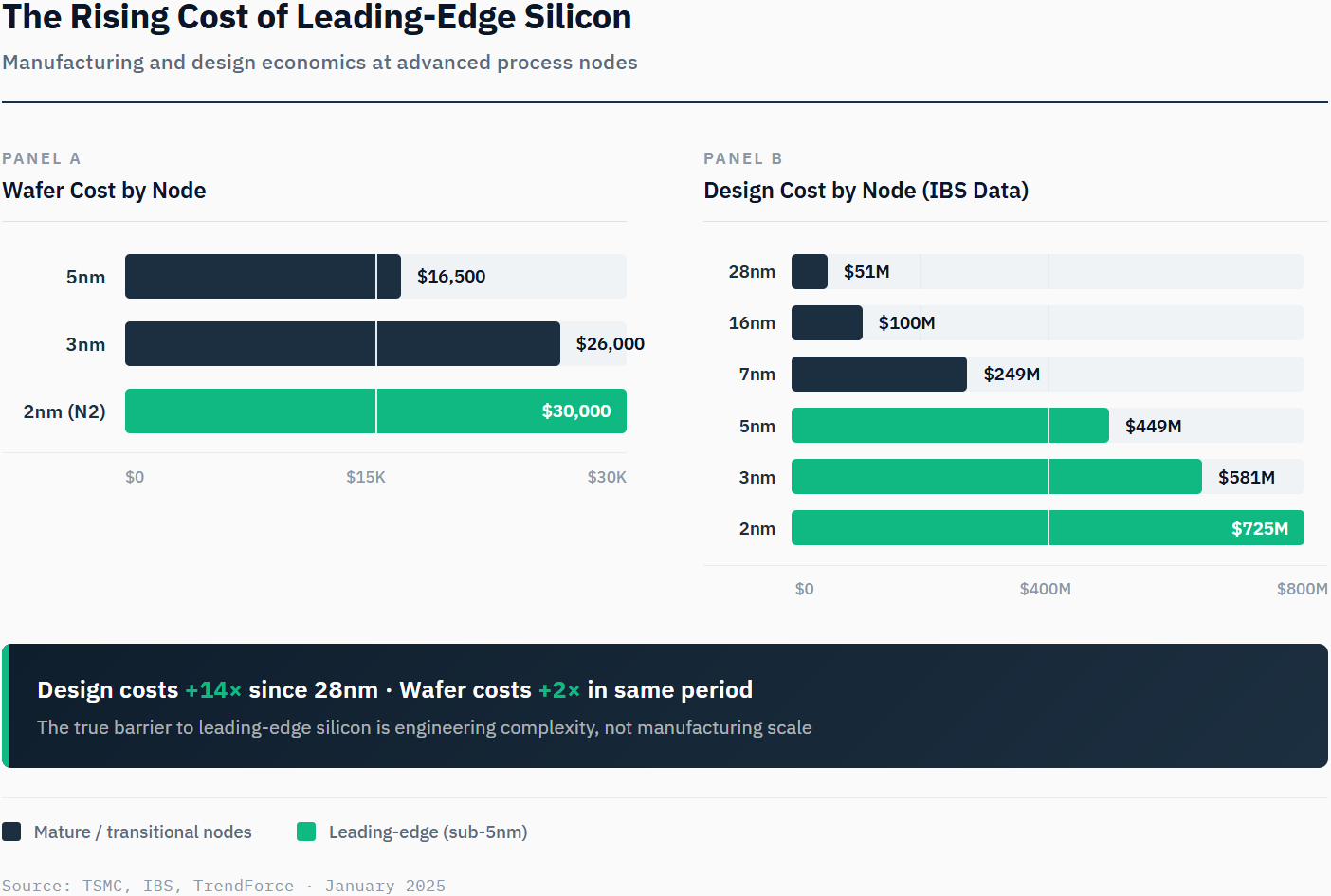
The economics of leading-edge semiconductors have crossed a threshold that restructures the entire industry. TSMC's 2nm wafers cost approximately $30,000 each—a significant increase over 3nm pricing and roughly double the cost at 5nm. But wafer pricing tells only part of the story.
According to IBS data, designing a chip at the 2nm node costs $725 million before a single transistor is etched. That figure includes EDA software licensing, IP blocks, verification, and the hundreds of engineers required to tape out a complex SoC. The trajectory is unmistakable: each node transition adds hundreds of millions in non-recoverable design expense. Software verification and validation alone now consume over 40% of that budget.
This is the first node where the economic justification shifts fundamentally. Previous shrinks delivered cheaper transistors. N2 delivers power efficiency—10-15% speed gains or 25-30% power reduction—but at higher cost per transistor. Companies aren't buying cheaper compute; they're buying compute that fits within a power envelope. That's a different value proposition entirely.
The cost structure creates a brutal volume threshold. To amortize $725 million in design costs across a product's lifecycle, a company needs guaranteed volume in the tens of millions of units—or margins so extraordinary that lower volumes still make financial sense. Apple's iPhone shipments exceed 200 million annually. Nvidia's data center GPUs command $30,000+ average selling prices. These companies can absorb the entry fee. Most cannot.
The capacity allocation tells the story. Apple secured over 50% of TSMC's initial N2 capacity for its A20 mobile processor and M6 Mac silicon. Qualcomm and MediaTek, despite being major TSMC customers, are relegated to the N2P variant (a performance-enhanced iteration arriving later in the production cycle). AMD, Nvidia, and the hyperscaler custom silicon teams compete for remaining allocation.
Samsung's struggles compound TSMC's leverage. After three years of 3nm production, Samsung's commercial logic yields reportedly sit at 10-20%—meaning the vast majority of chips fail quality testing—so poor that Samsung purchased 100% of its Galaxy S25 chips from Qualcomm rather than use its own Exynos 2500. The competitive landscape has been permanently reshaped.
The cost barriers are now clear. But where do the companies priced out redirect—and what does that tell us about where value is migrating?
The companies priced out of leading-edge lithography aren't disappearing—they're pivoting. And that pivot is reshaping where value accrues in the semiconductor supply chain.
The binding constraint isn't wafer capacity. It's advanced packaging. TSMC's CoWoS (Chip-on-Wafer-on-Substrate) technology—required for integrating AI accelerators with high-bandwidth memory—is fully booked through 2026. Nvidia has secured approximately 60% of global CoWoS capacity—like locking in reservations at the world's most exclusive restaurant years in advance. A company designing a competitive AI chip faces two queues: one for 2nm wafers, another for packaging. Nvidia's packaging lock is as strategically significant as its GPU architecture.
This dynamic redirects capital from the fab to the packaging sector. ASE Technology, the world's largest outsourced semiconductor assembly and test provider, projects its advanced packaging revenue will more than double to $1.6 billion in 2025. Amkor's two-phase $7 billion advanced packaging campus in Arizona represents the largest packaging investment in U.S. history. These aren't incremental expansions. They're strategic repositionings to capture value migrating away from leading-edge fabrication.
The EDA (electronic design automation) duopoly benefits regardless of which path companies choose. Cadence and Synopsys together control roughly 60-70% of the chip design software market. Whether a customer designs a monolithic 2nm chip or a complex multi-chiplet package, they need the same verification, simulation, and physical design tools. Complexity is their tailwind—design costs rising faster than wafer costs means EDA vendors capture an increasing share of the total investment.
High-bandwidth memory (HBM)—the ultra-fast memory stacked directly onto AI chips—represents the next constraint after CoWoS. Approximately 85-90% of HBM production is dedicated to AI accelerators, with supply fully committed through 2026. Hyperscalers have pre-secured capacity across the entire advanced packaging stack, not just CoWoS.
The bifurcation creates distinct competitive dynamics. In the "sovereign tier"—companies that can access and afford 2nm plus advanced packaging—the battle is for capacity allocation and time-to-market. In the "legacy stratum"—everyone else—the competition shifts to packaging innovation, system integration, and design efficiency. The two echelons will increasingly operate as separate markets with different success metrics, different supply chain dependencies, and different investment profiles.
A seductive narrative has taken hold in semiconductor circles: advanced packaging and chiplet architectures democratize access to high performance. If leading-edge lithography is too expensive, the argument goes, companies can simply combine older-node tiles into competitive products. The playing field levels. Moore's Law continues by other means.
The narrative contains a kernel of truth wrapped in dangerous oversimplification.
Chiplet architectures do enable performance gains without node shrinks. AMD's success with its Zen processors—combining compute and I/O chiplets across different nodes—demonstrates the model works. The technology is real.
But the equalizer thesis ignores three structural realities.
First, advanced packaging has its own capacity constraints. TSMC's CoWoS is fully booked through 2026, expanding from roughly 75,000 wafers per month to 127,000 by year-end—yet demand continues to outpace supply. Nvidia, AMD, and the hyperscaler custom silicon programs have already secured multi-year allocations. A company "pivoting to chiplets" doesn't escape the queue—it joins a different one.
Second, advanced packaging carries substantial cost. While design costs are lower than monolithic 2nm, the manufacturing premiums are significant. These methods require specialized silicon layers to connect chips, precision bonding techniques, and managing quality across multiple individual chips that must work together perfectly. ASE and Amkor aren't building billion-dollar facilities because margins are thin. The cost advantage versus leading-edge is real but narrower than the narrative suggests.
Third—and most strategically important—the sovereign tier isn't standing still. Apple's M-series Ultra chips combine leading-edge logic with advanced packaging. Nvidia's Blackwell architecture integrates cutting-edge compute with CoWoS packaging and HBM memory stacks. The companies that can afford 2nm will use it *in combination* with chiplet approaches, compounding their advantage rather than ceding it.
The cyclical lens compounds the confusion. Semiconductor bears argue that packaging equipment demand—like all semi equipment—follows boom-bust patterns. When the current AI investment cycle peaks, they predict, advanced packaging will collapse alongside everything else.
This framework misses a structural shift. Traditional packaging serves consumer electronics companies managing quarterly inventory. Advanced packaging for AI serves hyperscalers making decade-long infrastructure commitments. Nvidia has booked production through 2028. Amazon's Trainium roadmap extends similarly. These aren't speculative orders that evaporate in a downturn.
The "chiplets democratize everything" thesis isn't wrong about the technology. It's wrong about the economics. Advanced packaging creates a viable alternative for companies priced out of 2nm—but it doesn't eliminate the stratification. It institutionalizes it. The legacy tier can compete within its stratum. It cannot bridge the gap to the sovereign echelon.
Understanding this distinction is essential for capital allocation.
The semiconductor industry's two-tier structure isn't a temporary condition awaiting normalization. It's the new equilibrium.
For the sovereign tier—Apple, Nvidia, AMD, and the hyperscaler silicon teams—the strategic imperative is capacity security across both wafers and packaging. TSMC allocation determines product roadmaps. These companies will pay premium prices and commit capital years in advance to maintain access. Their competitive moat is partially technological, but increasingly logistical.
For the legacy tier—mid-market processors, automotive, industrial, IoT—the game changes entirely. Performance differentiation comes through packaging innovation, system integration, and design efficiency rather than transistor density. The value chain shifts toward packaging specialists like ASE and Amkor, and toward EDA vendors whose tools enable chiplet complexity. Companies that recognize this transition early will find opportunities; those expecting lithography access to normalize will be structurally disadvantaged.
The investment implications follow the constraints. TSMC's pricing power at 2nm reflects near-monopoly economics—Samsung's yield struggles and Intel's foundry credibility issues leave no alternatives at scale. Intel 18A, while technologically promising with its PowerVia backside power delivery, has yet to secure foundry commitments from major external customers—Qualcomm and Nvidia continue directing new designs to TSMC. Until Intel demonstrates production-scale traction, TSMC's position remains uncontested. The EDA duopoly captures value regardless of which tier a customer occupies, with complexity driving license expansion.
One objection merits addressing: doesn't Taiwan geopolitical risk undermine the value of TSMC allocation? Counterintuitively, it reinforces it. Companies that have already secured TSMC capacity—and locked in packaging slots through 2026 and beyond—become *more* advantaged precisely because new entrants face even higher barriers. Meanwhile, China's mature-node capacity expansion creates pricing pressure on legacy nodes but operates in an entirely parallel market, irrelevant to the leading-edge dynamics described here.
The filter has been applied. The sorting has begun. Capital allocation in semiconductors now requires understanding not just who makes the best chips, but who secured their place in line.
The $30,000 wafer and $725 million design threshold represent verified, structural barriers that permanently segment the semiconductor market. The bifurcation is already visible in capacity allocation patterns—Apple's 50%+ N2 lock, Nvidia's 60% CoWoS dominance—and Samsung's commercial yield failures that forced Galaxy S25 to use competitor silicon. Rating 8.5 rather than 9.0+ reflects three uncertainties: (1) design cost estimates vary by chip complexity—$725M represents a complex SoC baseline, not a ceiling; (2) breakthrough packaging technologies could narrow tier performance gaps faster than anticipated; (3) Intel 18A remains an uncertain variable, though current external customer traction suggests limited near-term impact. The core thesis—permanent bifurcation requiring different competitive strategies—carries high conviction.
This commentary is provided for informational purposes only and does not constitute investment advice, an offer to sell, or a solicitation to buy any security. The information presented represents the opinions of The Stanley Laman Group as of the date of publication and is subject to change without notice.
The securities, strategies, and investment themes discussed may not be suitable for all investors. Investors should conduct their own research and due diligence and should seek the advice of a qualified investment advisor before making any investment decisions. The Stanley Laman Group and its affiliates may hold positions in securities mentioned in this commentary.
Past performance is not indicative of future results. All investments involve risk, including the potential loss of principal. Forward-looking statements, projections, and hypothetical scenarios are inherently uncertain and actual results may differ materially from expectations.
The information contained herein is believed to be accurate but is not guaranteed. Sources are cited where appropriate, but The Stanley Laman Group makes no representation as to the accuracy or completeness of third-party information.
This material may not be reproduced or distributed without the express written consent of The Stanley Laman Group.
© 2025 The Stanley-Laman Group, Ltd. All rights reserved.
SLG is an independent investment management and advisory firm serving ultra-high-net-worth individuals, families, and institutions.